12
People
4
Projects
Transducer materials are functional materials that convert one form of energy into another. They are essential to technologies such as sensors, actuators and radiofrequency (RF) components. These applications are becoming increasingly critical in the context of modern technological demands, which include:
Beyond traditional applications, ferroelectrics can also convert different types of energy into chemical energy and serve as catalysts in redox reactions, for example water splitting to produce green hydrogen.
A set of interrelated challenges must be addressed to enable the next generation of transducer technologies:
The main objective of the Chemical Processing of Transducer Materials is to lead the research and development of transducer materials through innovative chemistry-based processing techniques. With a strong background in ferroelectric materials, the group aims to create scalable and cost-effective solutions for next-generation electronic devices and beyond. It is also committed to fostering doctoral education and advancing knowledge through collaborations with academic and industrial partners.
Piezoelectric haptics
Piezoelectric haptic technologies offer high-quality and fast response vibrotactile feedback. Piezoelectric actuators generate ultrasonic vibrations in a plate (such as a screen), enabling real-time control of the friction coefficient between the finger and the surface as the finger moves across it. The group is developing advanced processing techniques, such as inkjet printing and flash lamp annealing, for the efficient integration of oxide thin-film piezoelectrics, including Pb(Zr,Ti)O₃, onto glass substrates. These structures are used in proof-of-concept haptic devices.
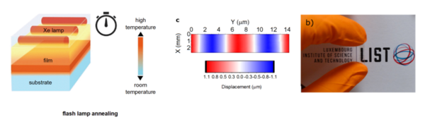
Figure 1. Left: Schematic diagram of flash lamp annealing. This method enables the direct integration of oxide piezoelectrics onto temperature-sensitive substrates. From: Cardoletti et al., Nat. Comm. 15, 1890 (2024). Middle: Out-of-plane displacement of a glass-based haptic device with integrated piezoelectric actuators. Right: Appearance of such device, demonstrating its transparency. From: Glinsek et al., Adv. Funct. Mater. 36, 2003539 (2020).
Lead-free piezoelectric materials
Lead-based piezoelectrics remain the benchmark for sensing and actuator applications due to their superior performance. However, their toxicity poses significant risks to both human health and the environment. The group is therefore exploring alternative lead-free thin-film piezoelectric materials. Current work focuses on (K,Na)NbO₃, which exhibits a strong piezoelectric response suitable for actuator applications, and on ferroelectric HfO₂ - an unconventional ferroelectric with moderate piezoelectric properties that shows promise for use in resonator devices.
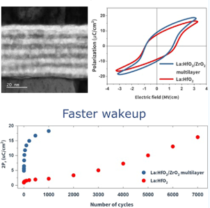
Figure 2. Scheme showing how multilayering improves the wake-up behaviour of HfO2-based ferroelectrics. From: Mandal et al. ACS Omega 10, 13141 (2025).
Printed temperature and strain sensors
Sensors play a vital role in advancing sustainability and improving quality of life. Unlocking their full potential requires the development of simple, low-cost fabrication technologies. The group focuses on temperature and strain sensors using printed conductive materials. Deposition techniques, such as inkjet and aerosol jet printing, are employed, followed by light-based thermal treatments including laser and flash lamp annealing. These sensors are targeted for use in structural health monitoring across a range of industries, including aerospace.
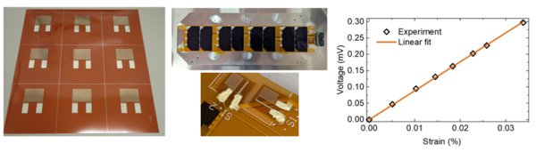
Figure 3. Left: An array of inkjet-printed sensors on a Kapton substrate. Middle: Printed strain sensors integrated into deployable solar panels. Right: Functional response of a printed strain sensor. From: Nouchokgwe et al., APL Electron. Dev. 1, 036117 (2025).
The electro-optic effect enables modulation of a ferroelectric film’s refractive index by applying an external electric field. This phenomenon is essential for controlling light transmission in optical chips, tunable photonic gratings and photon-based quantum processors.
In addition to conventional linear electro-optic effects, the group investigates extrinsic mechanisms, such as field-induced phase transitions and reversible ferroelectric domain switching, that produce significantly stronger responses. These enhanced effects open up opportunities for the further miniaturization of optics-based devices.
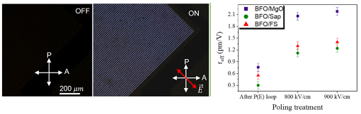
Figure 4. Left: Change-of-light transmission in a thin film of PbZrO3 due to a field-induced phase transition. From: Biswas et al., Phys. Rev. Mat. 9, L091403 (2022). Right: Three-fold increase of effective electro-optic coefficient reff in BiFeO3 on different substrates, i.e. magnesium oxide, sapphire and fused silica, due to reversible ferroelectric domain switching. From: Blazquez Martinez et al., Opt. Mat. Exp. 7, 2061 (2023).
In response to the growing demand for high-frequency electromagnetic devices operating in the millimetre-wave range and beyond, and driven by applications such as 5G/6G communications and remote sensing (e.g. automotive radar for autonomous vehicles), the group focuses on two key areas:
(1) printing conductive materials, including transparent indium tin oxide (ITO) and various metals, for antenna fabrication;
(2) developing ferroelectric substrates with ultra-high, electrically tuneable dielectric permittivity, such as Pb(Zr,Ti)O₃ on glass. The overarching goals are to enable seamless integration of antennas into a wide range of objects, and to further miniaturize devices, thereby enhancing their functionality.
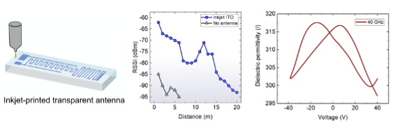
Figure 5: Left: Scheme of a transparent Bluetooth antenna. Middle: RSSI (Received Signal Strength Indicator) of the invisible antenna, demonstrating its usability for short-range communications. From: Glinsek et al., Cell. Rep. Phys. Sci. 4, 101685 (2023). Right: Voltage-dependence of dielectric permittivity of Pb(Zr,Ti)O3 thin film measured at 40 GHz.
Green hydrogen, which is produced via water electrolysis powered by renewable energy, has emerged as a sustainable energy solution that is clean, reliable and resilient to future challenges. However, its high production cost limits its share in global hydrogen output.
Ferroelectric materials are increasingly recognized as multifunctional catalysts capable of converting abundant energy sources, such as solar, thermal and mechanical energy, into chemical energy. The group investigates and optimizes ferro-catalytic processes for water-splitting reactions, with current research focusing on materials such as BiFeO3, Pb(Sc,Ta)O3 and (Ba,Sr)TiO3.


Konsago S.W., Koblar M., Žiberna K., Matavž A., Mandal B., Glinšek S., Bobnar V., Benčan A., Malič B.
Journal of Alloys and Compounds, vol. 1047, art. no. 185124, 2025
Highly transparent lead-free piezoelectric haptic device
Song L., Glinsek S., Alluri N.R., Kovacova V., Melchiorr M., Martinez A.B., Mandal B., Cardoletti J., Defay E.
Communications Materials, vol. 6, n° 1, art. no. 91, 2025
Ti-doped Pb(Sc0.5Ta0.5)O3thin films for non-linear pyroelectric energy harvesting
Aravindhan A., Glinsek S., Granzow T., Song L., Nouchokgwe Y., Kovacova V., Defay E.
Ceramics International, vol. 51, n° 25PC, pp. 47264-47271, 2025