15
People
16
Publications in 2024
8
Projects
Today’s rapidly evolving, data-driven world requires advanced sensing technologies that are ultra-miniaturized, energy-efficient and seamlessly connected to Internet-of-Things (IoT) systems. These sensors must be capable of tackling complex, real-world challenges across a range of applications. Chemo-sensors, in particular, play a vital role in driving progress in key areas such as environmental monitoring, the energy transition and healthcare. For example, sensing technologies can make a difference in:

Rapid urbanization, industrialization, widespread close working conditions and climate change, contribute to increased exposure to airborne pollutants, which in turn impact people’s health and wellbeing worldwide. Poor indoor and outdoor air quality can result in eye irritation, dry throat, asthma and lung inflammation, and in the long run, may lead to respiratory and cardiovascular diseases. These conditions are driven by outdoor pollutants, such as traffic-related emissions and volatile organic compounds from industry as well as indoor ones, as well as indoor pollutants such as formaldehyde and chemicals released from building materials.

The healthcare sector is undergoing a major transformation, driven by the need for non-invasive health monitoring and early diagnostics. Breath analysis is an example of a potentially powerful non-invasive diagnostic tool providing health status information based on the presence of specific gases and other biomarkers in the exhaled breath, which are related to metabolic and respiratory conditions such as diabetes, asthma and gastrointestinal disorders.

In the context of energy transition beyond fossil fuels, the adoption of hydrogen-based solutions for transportation and energy storage raises safety concerns due to the explosive nature of this chemical compound. Social acceptance would increase if monitoring solutions were adopted accompanying the diffusion of hydrogen infrastructures, enabling early leakage detection and target safety improvements.

Advances in understanding proteins and their interactions with other molecules are accelerating transforming both the healthcare and biotechnology sectors. As new applications emerge in these fields, there is a growing demand for sensors capable of handling the complexity of biomolecules. These advances are paving the way for more accurate diagnostic tools, personalized vaccines and new types of antibiotics. At the same time, they are opening new possibilities in biotechnology, including the development of smart biomolecules that can bind to specific materials, benefiting industries like chemical manufacturing and environmental monitoring.
All this calls for the development of advanced sensing technologies that are not only ultra-miniaturized and energy-efficient, but also capable of managing the complexity of such applicative scenarios by taking advantage of 5G/6G-supported IoT connectivity and AI data processing.
The Nanostructured Multifunctional Materials for Sensing group aims to tackle these challenges by creating next generation sensing solutions. The group harnesses expertise in materials science, nanotechnology, microelectronics and microfluidics to design and develop micro- and nanostructures with customized electrical and optical properties serving as active components in gas and bio-sensing microdevices. Research covers oxide nanostructures, semiconductor heterostructures, 2D materials, plasmonic arrays, multilayers, and compact and nanogranular thin films, as well as their combinations targeting smart materials with novel functionalities. The group also designs and develops lab-on-a-chip systems that integrate microfluidics and electrochemical sensing technologies to screen and analyze peptide interactions, with the aim of advancing AI-driven drug discovery, vaccine developments and material-specific binders.
The ambition of the group is to translate fundamental discoveries and knowledge advancement in materials science and condensed matter physics into real-world applications that positively impact health, wellbeing and environmental sustainability, building a pipeline from low Technology Readiness Levels (TRL 1-4) to deployment-ready technologies (TRL 5-7) in collaboration with industrial partners. Key development lines include:

The group develops ultra-miniaturized, low power consumption gas sensor arrays integrated with AI algorithms and IoT connectivity (5G/6G), aiming to provide reliable solutions for the detection and monitoring of airborne chemicals. Targeted applications include: (1) indoor and outdoor air quality monitoring networks featuring real-time pollution maps for citizen awareness, smart city planning and optimized air conditioning systems; (2) portable breath analyzers trained with AI to detect metabolic biomarkers such as NO, NH₃, CH₄ and acetone, as non-invasive diagnostics for conditions like asthma, diabetes and gastrointestinal disorders; (3) detection of emissions of specific chemicals with environmental and safety concerns, such as fluorinated compounds with a high global warming potential (GWP) and hydrogen.
Reference projects: AMUSENS (Horizon Europe), GASENSE (FNR), NANOSENSE (ESA).
The group develops next-generation lab-on-chip technologies aimed at transforming the detection and analysis of molecular interactions. This approach integrates innovations in micro- and nanotechnology, biochemical engineering and advanced sensing to create powerful tools for precision medicine. A key focus is the integration of peptide microarrays with label-free electronic sensors, including micro-controlled in-situ peptide synthesis, to enable the highly sensitive, real-time detection of interactions such as peptide-protein binding. Central to this platform are semiconductor field-effect transistors built with high-k dielectrics and novel 2D materials, which provide the sensitivity and scalability needed for future biomedical applications. This fusion of molecular diversity and electronic precision opens new frontiers in AI-driven diagnostics and therapeutic discovery, advancing the capabilities of biotechnology and healthcare.
Reference projects: ELECTROMED (EIC), PROFET-SEQ (FNR), NANOTRAACES (M-ERA.NET).
The group engineers the structure and functionality of material interfaces at molecular length scales (a few to several tens of nanometres) to drive the high-performance interrogation or control of biological interactions, involving biomolecules or biological cells, on material interfaces. These efforts draw on our expertise in scalable, high-throughput, cost-effective approaches for the nanofabrication of well-defined nanoarrays (of metal, metal-oxide, polymers or organic molecules) on full wafers and beyond. It also fosters the integration of nanostructures into diverse form factors, including microfluidic lab-on-chip, plastic, paper, microarrays, microcarriers in personalized healthcare diagnostics and therapy applications, bioimplants, and antimicrobial food packaging applications. These efforts are readily transferable to other contexts where detecting, quantifying or manipulating molecule-material interactions is important, such as defence, environment, security and outer space.
Reference projects: A-BLOCK (EU PRIMA), BIOFLICS (FNR), NANOSENS (FNR).
To accomplish the group’s objectives, we combine core competences, expertise, and cutting-edge, unconventional instrumentation. The main capabilities include:
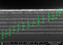
The group manages a range of equipment, including three reactors from Applied Materials and Beneq interfaced with ISO 4 cleanroom. Over the years, it has amassed an ALD material portfolio comprising oxides (e.g. Al2O3, ZnO, TiO2, SnO2, HfO2, ZrO2, SiO2, Y2O3), nitrides (e.g. AlN, GaN), metals (e.g. Ni, Ag, Pt), and their combinations in multilayered structures. The full conformity of ALD coatings enables the group to treat industrial parts with complex 3D geometry (e.g. hollow volumes, high aspect ratio elements), with detail down to the micrometric scale.
For more information, see here:
Strategies for Enhancing the Electrocatalytic Performance of Transition Metal Thin Films Deposited via Chemical Vapor Process for Hydrogen Cells and Electrolysers. ChemElectroChem 2025. https://doi.org/10.1002/celc.202400609
Conformal Chemical Vapor-Phase Deposition of Ultra-Thin Conductive Silver Films. ACS Appl. Mater. Interfaces 2020. https://doi.org/10.1021/acsami.0c08606
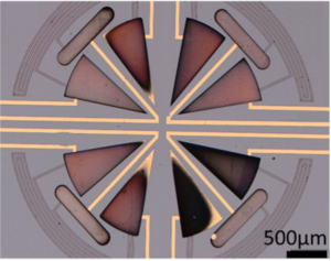
With a deposition area as large as 45 cm diameter and up to six different Knudsen evaporation sources operating at the same time, the CBVD facility leverages the combinatorial composition of metal-organic molecular beams to produce stoichiometry gradients across the deposition area. This enables a continuum of different materials to be obtained in one single deposition session. The group works on the multiple doped perovskites NaTaO3 and SrTiO3.
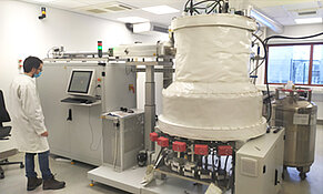
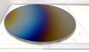
The photos illustrate the CBVD reactor and an example of deposition on a 45 cm diameter wafer where the colour is related to the composition gradient (not to the thickness).
For more information, see here:
SrTiO3 thin film photoanodes fabricated by combinatorial chemical beam vapour deposition. J. Mat. Chem. 2024. https://doi.org/10.1039/D3TA07695D
Vanadium and strontium doping in dual-doped sodium tantalate thin films. Sustain. Mater. Technol. 2024. https://doi.org/10.1016/j.susmat.2024.e01006
Widely tuneable composition and crystallinity of graded sodium tantalate. Nanomat. 2022. https://doi.org/10.3390/nano12061012
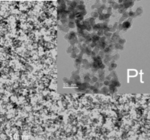
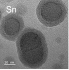
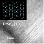
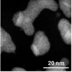
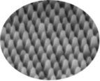
Operating on 2 mm diameter rod metallic targets, the group’s prototype system for SCBD performs room-temperature deposition of nanogranular films via the soft assembling of atomic clusters / nanoparticles with dimensions of 1-5 nm. The material portfolio includes Ni, Zr, Pd, Sn, W, Pt, Au, and their combinations in bimetallic systems. In the image below, examples of nanogranular materials are shown: Pt, Sn-SnO core-shell particles, and intermetallic 2D layered phase PtSn4 (high and low magnification).
For more information, see here:
Supersonic cluster beam deposition of bimetallic Sn–Pt nanogranular films: nanostructure control, segregation, and 2D intermetallic phases. Nanoscale Advances 2025. https://doi.org/10.1039/d5na00683j
Core–shell structure in single Sn/SnOx spherical nanoparticles. Applied Surface Science 2025. https://doi.org/10.1016/j.apsusc.2024.161984
The role of coalescence and ballistic growth on in-situ electrical conduction of nanostructured Sn films. Applied Surface Science 2024. https://doi.org/10.1016/j.apsusc.2024.160268
Intermediate tin oxide Sn3O4 in stable core-shell structures. Applied Surface Science 2024. https://doi.org/10.1016/j.apsusc.2024.159846
Supersonic Cluster Beam Deposition for the integration of functional nanostructured films in devices. Springer-Nature Switzerland AG, 2024. https://doi.org/10.1007/978-3-031-42700-8
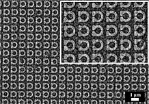
In collaboration with other units at LIST, the group makes the most of the liquid-phase synthesis and integration of metal-oxide nanostructures (ZnO, CuO, SnO2) and nanowires (ZnO, Ag) into electronic and opto-electronic devices, including gas sensors and photodiodes, by spray deposition, inkjet printing and aerosol jet printing.
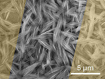
Above, an example of CuO bundles that have been synthetized and deposited on gold electrodes to form a conductive network with gas sensing properties, a multi-pixel gas sensor based on four different materials integrated on a single chip, and a micro-hotplate batch coated with ZnO nanowires, are shown.
For more information, see here:
Morphology control of copper hydroxide based nanostructures. J. Cryst. Growth. 2021. https://doi.org/10.1016/j.jcrysgro.2021.126225
Spray Deposition of Silver Nanowires on Large Area Substrates for Transparent Electrodes. ACS Appl. Nano Mater. 2021. https://doi.org/10.1021/acsanm.0c02763
Aspect ratio improvement of ZnO nanowires. Cryst. Eng. Comm. 2016. http://doi.org/10.1039/C6CE00904B
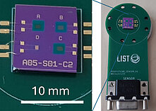
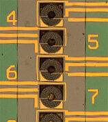
The group investigates the electronic, thermoelectrical, optical and gas diffusion properties of thin films and nanomaterials with the aim of understanding specific charge/mass transport mechanisms, energy dissipation and light–matter interactions in nanoscale systems. Its characterization capabilities include Hall effect measurements, the Seebeck coefficient analysis, spectroscopic ellipsometry, UV-Vis-NIR absorption and Kelvin probe techniques. The group uses this expertise to correlate material structure and composition with key physical properties, supporting the development of high-performance coatings and devices for sensing, energy and transparent electronics applications.
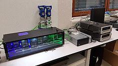
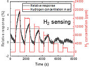
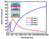
The photograph above shows our gas sensing test bench, an example of hydrogen sensing measurements (at room T) and an example of multilayer coating with tailored optical properties.
For more information, see here:
On the charge transport models in high intrinsic defect doped transparent and conducting p-type Cu–Cr–O delafossite thin films. J. Phys. D: Appl. Phys. 2025. https://doi.org/10.1088/1361-6463/ad800d
Electrical properties of strained off-stoichiometric Cu–Cr–O delafossite thin films. J. Phys.: Condens. Matter 2024. https://doi.org/10.1088/1361-648X/ad2a07
Haze factor of silver nanowires in variable refractive index environment. Nanotechnology 2024. https://doi.org/10.1088/1361-6528/ad59ae
Oxygen Adsorption and Desorption Kinetics in CuO Nanowire Bundle Networks: Implications for Mox-Based Gas Sensors. ACS Appl. Nano Mater. 2022. https://doi.org/10.1021/acsanm.2c01245
Detection mechanism in highly sensitive ZnO nanowires network gas sensors. Sens. Act. B: Chem. 2019. https://doi.org/10.1016/j.snb.2019.05.079
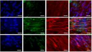
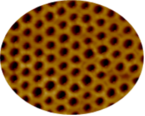
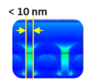
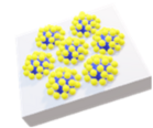
The group develops nanoplasmonic sensors that harness light-matter interactions at sub-10nm electromagnetic hotspots for the detection of small (metabolite, drugs or other) or large (bio) molecules using surface-enhanced Raman spectroscopy (SERS), metal-enhanced fluorescence (MEF), localized or planar surface plasmon resonance (LSPR, or SPR)-based refractive index sensing. It nanoengineers the surface structure and functionality to control analyte mass transport and analyte capture, and steer the behaviour of mammalian or bacterial cells using nano-QCM. This process includes building innovative multimodal tools that provide complementary information about the molecular interactions at a specific point on the material. The group integrates these sensing techniques into microdevices that control over fluid management, multiplexing, spectral identification and quantification of molecular interactions.
For more information, see here:
Interplay of Surface Nanotopography and Tether Flexibility Towards Analyte Capture by Tethered Receptors. Sensors and Actuators Reports 2025. https://doi.org/10.1016/j.snr.2025.100388
Plasmonic Microcarriers for Sensing and Cell Expansion. Sensors and Actuators Reports 2023, https://doi.org/10.1016/j.snr.2023.100173
Confined Adsorption within Nanopatterns As Generic Means to Drive High Adsorption Efficiencies on Affinity Sensors. Sensors and Actuators B: Chemical 2022. https://doi.org/10.1016/j.snb.2022.131945
Mesenchymal Stem Cell Differentiation Driven by Osteoinductive Bioactive Nanoscale Topographies. Applied Science 2021. https://doi.org/10.3390/app112311209
Hierarchically Structured Plasmonic Nanoparticle Assemblies With Dual-Lengthscale Electromagnetic Hot-Spots For Enhanced Sensitivity in Detection Of (Bio)Molecular Analytes. J. Phys. Chem. C 2021. https://doi.org/10.1021/acs.jpcc.0c10467
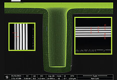
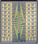
The group has developed micromachined electrochemical reactor arrays coupled with microfluidics and equipped with label-free field-effect sensors based on high-k dielectrics and graphene. This lab-on-a-chip platform is validated according to the synthesis of peptide sequence arrays with in-situ, real-time control of the process.
For more information, see here:
Optimizing peptide detection using FET-based sensors: Integrating non-linearities of surface functionalization. Solid-State Electronics 2025. https://doi.org/10.1016/j.sse.2025.109161
Assessment of ion-sensitivity of Si3N4 based feedback field effect transistor using snap-back characteristics. Solid State Electronics 2025. https://doi.org/10.1016/j.sse.2025.109159
Acid-Modulated Peptide Synthesis for Application on Oxide Biosensor. Nanomaterials 2023. https://doi.org/10.3390/nano13243092
Miniaturized Control of Acidity in Multiplexed Microreactors. ACS Omega 2023. https://doi.org/10.1021/acsomega.2c06897
Universal control of proton concentration using an electrochemically generated acid compatible with miniaturization. Nanoscale Advances 2022. https://doi.org/10.1039/D2NA00275B
The development of functional micro- nanostructures, multilayers and microdevices within the group is supported by expertise in computational design and modelling. The group is at the forefront of recent advancements in multiphysics modelling and design, including multi-scale modelling, coupled physics simulations, reduced-order modelling, machine-learning integration and optimization. The team particularly leverages its competence in COMSOL Multiphysics.
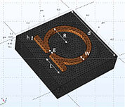
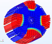
Above is an example of metamaterial design and production for optical applications, and of a cog-free electric microgenerator.
For more information, see here:
Spectroscopic Ellipsometry and Wave Optics: A Dual Approach to Characterizing TiN/AlN Composite Dielectrics. Crystals 2025. https://doi.org/10.3390/cryst15020143
Multi-physical modelling, design optimization and manufacturing of a composite dielectric solar absorber. Composites Part C 2022. https://doi.org/10.1016/j.jcomc.2022.100282
EM modelling of arbitrary shaped dispersive chiral dielectric objects using a 3D leapfrog scheme on unstructured meshes. Computational Mechanics 2020. doi.org10.1007/s00466-020-01930-1
An intuitive computational multi-scale methodology and tool for the dynamic modelling of viscoelastic composites and structures. Composite Structures 2016. https://doi.org/10.1016/j.compstruct.2016.02.032


Electrochemically-enabled high-throughput peptidomics for next generation precision medicine
Transparent gas permeation barrier on polymer foils for packaging and flexible electronics
Developing new biomaterials for proliferation and in vitro expansion of stem cells
Moreira M., Fleming Y., Grysan P., Vergne C., Philippe A.M., Lunca-Popa P.
Journal of Materials Science, vol. 61, n° 4, pp. 2380-2395, 2026
Peptide-Based Plasmon-Enhanced Spectroscopic Immunoassay to Detect Immunity Against Cytomegalovirus
Chandra Singh A., Sidhoum C., Payen H., Balakrishnan D., Juodkazis S., Østerbye T., Krishnamoorthy S.
Biosensors, vol. 15, n° 12, art. no. 817, 2025
Beggiato M., Payen H., Krishnamoorthy S.
Sensors and Actuators Reports, vol. 10, art. no. 100388, 2025